Upgrade Your CMP Semiconductor Process with Foam Solutions

Semiconductors are important components for many applications and manufacturing processes. As their importance for the industry is growing and there are strong dependencies, there is a high demand, and shortages can have serious consequences. In addition, a shift in semiconductor technology from Silicon (Si) to Silicon Carbide (SiC), mainly driven by the electric vehicle industry, as well as a growing need for analogue instead of microcontroller units (MCU), is changing the semiconductor landscape.
As the industry is changing rapidly, are you struggling to keep up with the demand for semiconductors in your industry?
With shortages costing the global economy billions of pounds, improving manufacturing processes has never been more important. As a result, new production capabilities across the globe are currently being built and, in addition to these more decentralised factories, new and more efficient production technologies are being developed and implemented.
One of these technologies with potential for optimisation is the chemical mechanical planarisation (CMP) process, where special foams are used to remove excess material from the surface of the wafer during fabrication. In this article, we'll explore the role of foam solutions in CMP semiconductor processes and how they can be used to streamline manufacturing and improve efficiency. By the end, you'll have a better understanding of how innovative materials and small differences can make a big impact on your wafer production.

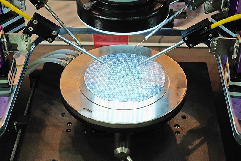
Chemical mechanical planarisation (or polishing) is a critical process in semiconductor manufacturing and it involves polishing the surface of a silicon wafer to a high degree of flatness. The process is used multiple times at each layer of the wafer to remove excess materials and ensure uniformity in the thickness and smoothness of the wafer surface.
But where does foam come into play? Foam pads are used in the polishing process in combination with slurry on a polishing tool. The slurry with abrasive particles and chemicals is applied to the wafer surface while it is rotated against a polishing pad. The foam is used as a carrier for the slurry and it helps to distribute the abrasive particles evenly across the wafer surface. The foam also provides a cushioning effect that helps to prevent damage to the wafer.
Furthermore, pads and slurries are consumables used in the CMP process and should be selected based on technical performance, process optimisation, and cost-of-ownership. But what are the criteria to consider for selecting ideal foam pads? Let us have a closer look.
When selecting foam materials for CMP processes, it’s important to consider factors such as the density, hardness, and compressibility of the foam. These properties can affect the polishing results and the lifespan of the foam pad. The questions you might have could be: Do I need a foam material that can withstand high temperatures or harsh chemicals? Am I looking to improve the efficiency of the polishing process? By understanding the properties of foam materials and exploring innovative solutions, you can optimise your CMP process and improve your wafer production.
There are very interesting innovations available that offer various advantages over standard materials.
As PFAS (per- and polyfluoroalkyl substances) materials are currently a significant supply chain risk for semiconductor manufacturers, Saint-Gobain® Tape Solutions is currently developing non-PFAS alternatives for the semiconductor market. Customers have requested high temperature, chemical resistant, inert, and hydrophobic materials to replace the fluoropolymers used today in gaskets and as part of the processing equipment.
Also, management of heat is a critical need for semiconductors. Saint-Gobain Tape Solutions provides a range of soft, thermally conductive TIM (Thermal Interface Material) pads that are used to help draw the heat away from sensitive components. As more energy is used in AI (artificial intelligence), more heat is generated, and there is a greater need for thermally conductive materials.
In addition, new foam materials are constantly being developed and tested to improve CMP processes. For example, researchers are experimenting with foam materials that have a higher thermal conductivity, which could improve the efficiency of the polishing process.
We have seen that special polishing pads in the CMP process can help to achieve higher levels of precision and uniformity, reducing the need for additional processing steps and minimising material waste. This can be one piece in the puzzle to improve semiconductor manufacturing efficiency. If you are working on optimising supplying high-end semiconductors to the industry, talk to your tape expert and see how special CMP foam pads can help.